Fabrication of Quantum Optical Devices Using Indium Phosphide Technology

Indium phosphide (InP) stands at the forefront of quantum optical device evolution. It is favored due to its distinct characteristics, perfect for crafting lasers, modulators, and photodetectors. In particular, photonic integrated circuits (PICs) are key areas of development, combining novel fabrication methods and photonics explorations on InP. This synergy is elevating quantum optics towards unparalleled levels of perproduction capabilities, miniaturization, and optimization in system cost, size, weight, and power (CSWaP).
InP's knack for merging active, like semiconductor optical amplifiers (SOAs), with passive components enables intricate and high-effectiveness photonic devices. These progresses are redefining the norms of precision, efficiency, and utility, symbolizing a significant step forward in the photonics sector.
Key Takeaways
- Indium phosphide (InP) is crucial for the development of quantum optical devices due to its unique material properties.
- Photonic integrated circuits (PICs) benefit greatly from InP, enabling the incorporation of both active and passive components.
- New fabrication techniques leverage InP to enhance system performance, miniaturization, and CSWaP optimization.
- InP-based components include lasers, modulators, and photodetectors, crucial for advanced photonic applications.
- InP enables the integration of active elements such as semiconductor optical amplifiers (SOAs) in photonic devices.
The Importance of Indium Phosphide in Quantum Optical Devices
Indium Phosphide (InP) emerges as a pivotal player in the quantum optical devices arena, heralding a new chapter in technological advancement. Its remarkable material qualities form the basis for major strides, especially in the realm of telecommunication and the fabrication of Photonic Integrated Circuits (PICs).
Material Properties and Characteristics
At the crux of Indium Phosphide lies an exceptional electron mobility, yielding unparalleled swiftness and efficiency in electronic and optical apparatus. This superior optical confinement further boosts the operation of active elements within PICs, thereby enhancing the precision of these devices. Noteworthy is its ability in integrating both active and passive components on a singular substrate, a feat that significantly advances the efficiency of these technologies.
Applications in Photonic Integrated Circuits (PICs)
For modern telecommunication to function optimally across extensive networks, the performance of InP PICs is indispensable. Their hybrid integration capability with silicon photonics significantly broadens the application horizon, making InP a choice selection in various critical sectors. Technologies such as Lidar, microwave photonics, and free-space laser communications benefit from the synergistic amalgamation of InP and silicon photonics, promising maximal operational efficacy.
Besides, InP's synergy with silicon nitride (SiN) presents a significant advancement potential for telecommunications and other photonics-powered domains. This strategic union ushers in the era of more resilient and versatile device architectures, paramount for the innovation trajectory of quantum optical technology. This underscores Indium Phosphide's role at the forefront of quantum optical innovation.
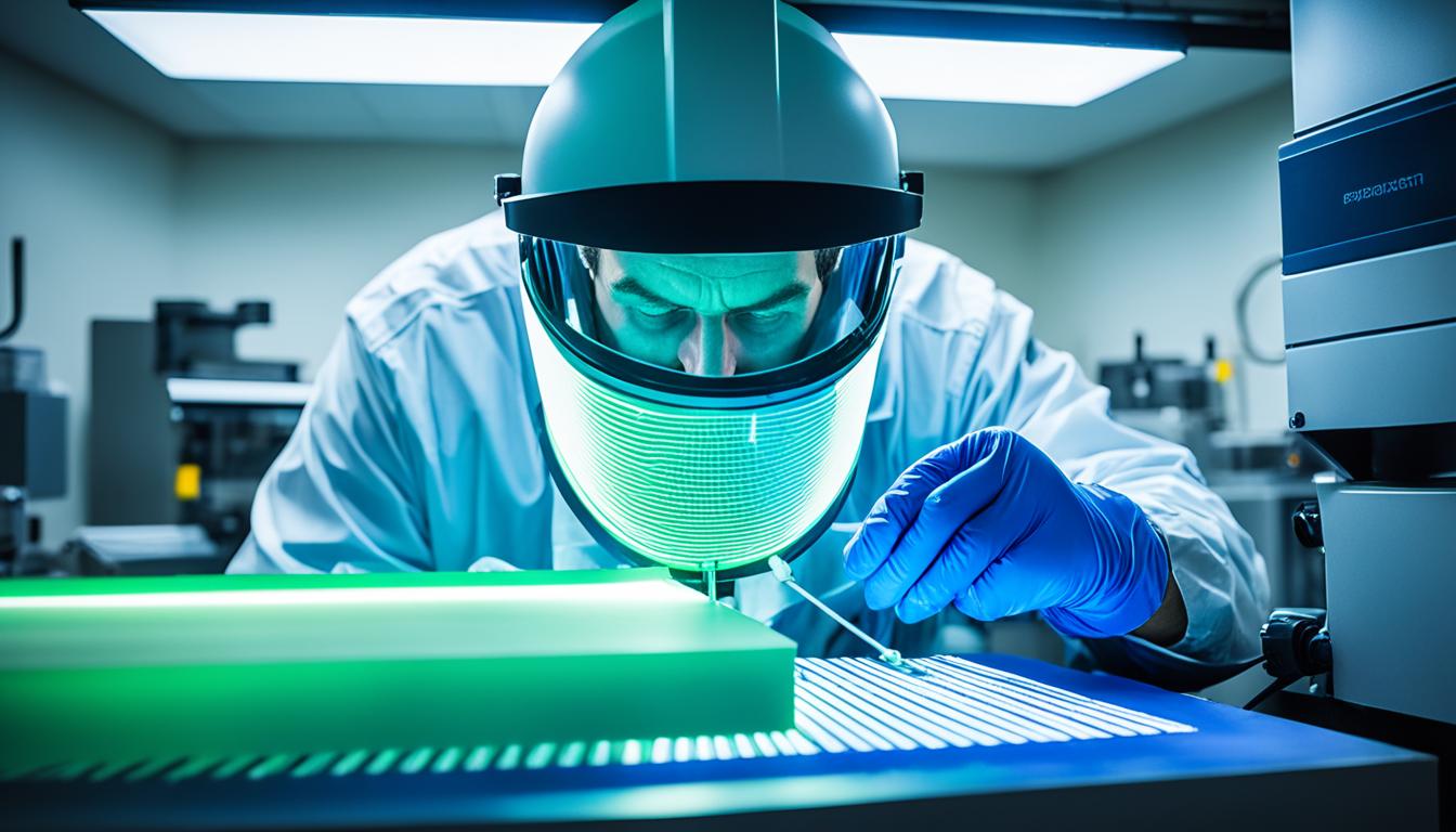
Advanced Coating Technologies for Indium Phosphide
The enhancement of InP devices depends significantly on advanced coating methodologies. Mainly, Metal Organic Chemical Vapor Deposition (MOCVD) and Molecular Beam Epitaxy (MBE) are instrumental in boosting the transmission speed and reliability of these devices. They are pivotal for achieving optimal InP attributes through accurate epitaxial layering.
Types of Coatings
The performance of InP devices is bolstered by a selection of coatings. These include dielectric coatings for optical control and metallic coatings to boost electrical conduction. Each kind of coating brings distinct advantages, meeting the specific needs of various applications and ensuring the efficiency and longevity of InP devices.
Impact on Performance
Coatings are crucial for the overall functionality of InP devices. Techniques like MOCVD and MBE allow for the precise control of epitaxial layering, which leads to enhancements in modulation speed and light emission. This precision is vital for applications demanding fast transmission, as seen in telecommunications and advanced photonic integrated circuits (PICs).
Indium Phosphide Epitaxy in Device Fabrication
Indium phosphide (InP) epitaxy plays a crucial role in manufacturing cutting-edge quantum optical devices. It involves the growth of epitaxial layers that form the basis for quantum well structures and other sophisticated components in these devices. These growth methods allow for precise engineering at the atomic level, ensuring the functionality and performance of the final product.
Metal Organic Chemical Vapor Deposition (MOCVD) Process
The Metal Organic Chemical Vapor Deposition (MOCVD) process stands out for its effectiveness in creating intricate epitaxial layers. This method employs metal-organic compounds to grow thin epitaxial films on surfaces, resulting in the production of uniform quantum well structures. An essential characteristic of the MOCVD technique is its capability to achieve high material quality while controlling the composition and thickness with great precision.
Furthermore, its adaptability has positioned it as the method of choice for incorporating various components in quantum devices. This flexibility is integral to ensuring the seamless integration of quantum wells, enhancing the overall efficiency and reliability of these technologies.
Molecular Beam Epitaxy (MBE) Techniques
Molecular Beam Epitaxy (MBE) stands as a key technology in epitaxial growth, renowned for its precision in material deposition. Leveraging the control over the flux of atomic beams, MBE enables the generation of epitaxial layers with accuracy measured on the atomic level. This attribute is fundamental in tailoring material characteristics for high-performance quantum optical devices. MBE excels in the production of uniform and defect-free quantum wells, a critical element in increasing the efficiency and reliability of devices.
Its ability to customize material properties at the atomic scale makes MBE indispensable for the sophisticated integration of quantum wells. This precision is vital for the advanced performance of these devices, aligning with the demands of quantum technologies.
The comparison between MOCVD and MBE techniques allows us to highlight specific advantages of each in epitaxial growth.
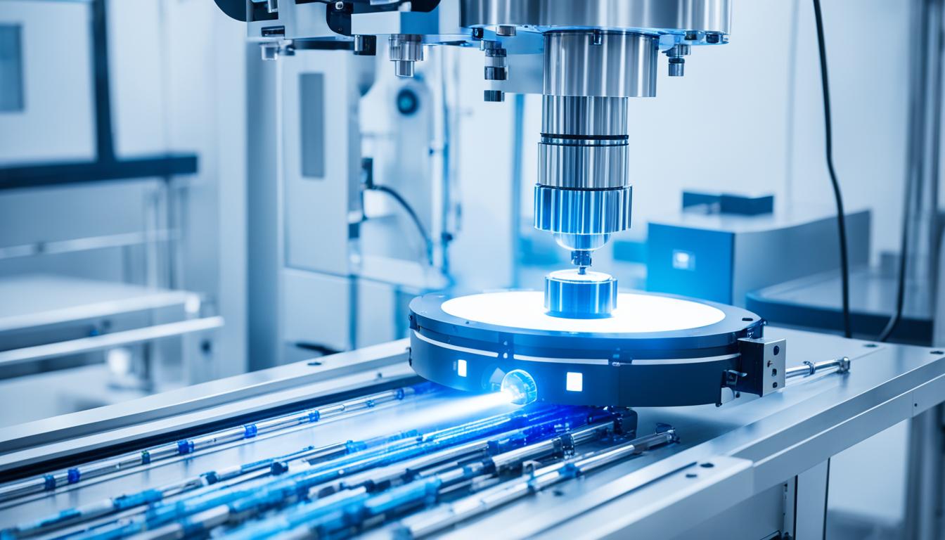
Role of Ion Beam Sputtering in Quantum Optical Device Production
Ion beam sputtering plays a pivotal role in crafting quantum optical devices by ensuring superior fabrication precision. It enables the uniform coating of target materials via the direction of ions. This leads to the production of high-quality thin films, imperative for quantum optics endeavors. Sputtering is paramount for the scalability and precision needed in these applications.
Process Overview
The process entails the targeted bombardment of a material with high-energy ions. This action ejects material atoms, leading to their deposition on a substrate, thereby forming a thin film. The technique offers a fine-grained control over layer attributes like thickness and composition, fundamental for the optical properties sought in waveguides and modulators.
Benefits and Challenges
Ion beam sputtering stands out for its unmatched precision in creating devices with a performance boost. It allows for depositing layers that are not only extremely thin but also uniform, which minimizes defects. Further, it supports the scalability of optical devices from lab research to commercial production.
Nevertheless, challenges exist, particularly in maintaining quality during mass manufacturing. The stability and repeatability of the sputtering process are key to ensure high performance and reliability at a larger scale. Addressing these challenges necessitates continual improvement in both equipment and process management.
Integration Techniques for Indium Phosphide Devices
The amalgamation of Indium Phosphide (InP) devices with various photonic materials stands as a cornerstone in augmenting device efficacy and expanding utility fields. Vanguard integration techniques, for instance, both hybrid and heterogeneous integration, spearhead pivotal strides in communication and sensing sectors. These methodologies transcend traditional paradigms, fostering revolutionary advancements.
Hybrid Integration with Silicon Photonics
Hybrid integration capitalizes on the strengths of both InP and silicon photonics, harmonizing their benefits. Through silicon photonics compatibility with InP's exceptional optoelectronic features, it achieves a harmonious material meld. Resultantly, it ushers in the era of highly efficient, economical photonic circuits. The-dimensional benefits of this convergence significantly ameliorate system costs, compactness, and energy utilization.
Heterogeneous Integration Strategies
Contrariwise, heterogeneous integration marks a quantum leap by amalgamating divergent material compositions and devices into unified entities. This method affords unparalleled versatility, pushing past the barriers of hybrid integration. It enables the marriage of InP with substrates like silicon nitride (SiN), elevating device prowess over extensive application spectra.
The symbiosis of both methodologies marks a watershed in the photonics domain, underlining the pivotal role of integration techniques in evolving InP device potentials.
Fabrication Process of Indium Phosphide Photonic Integrated Circuits
Indium phosphide photonic integrated circuits (InP PICs) stand at the forefront, transforming the photonics sector with unmatched efficiency and performance. The manufacturing journey is marked by a meticulous series of sequential steps. These steps guarantee the execution of every detail, leading to the pinnacle of production outcomes.
Step-by-Step Fabrication Workflow
The development of a photonic integrated circuit entails numerous key phases crucial for generating devices of superior quality; these phases encompass:
- Epitaxial Wafer Creation: Its genesis involves stacking multiple indium phosphide layers on a substrate to formulate an epitaxial wafer.
- Lithography: By applying advanced lithography, intricate patterns of PIC components are imposed onto the wafer.
- Etching: An accurate etching process unveils the photonic structures by selectively removing materials from the wafer.
- Metallization: The subsequent step incorporates depositing conductive metals to establish electric pathways within the PIC.
- Assembly: It culminates in the integration of the active and passive parts, culminating in the assembly of the PICs into their final, functional form.
Quality Control Measures
Maintaining the premium performance and dependability of photonic integrated circuits commands rigorous adherence to quality control within photonics. This overarching goal is achieved through:
- Process Monitoring: A continual supervisory regimen across all manufacturing phases to swiftly identify and rectify any aberrations.
- Optical Testing: Elaborate evaluation of the optical attributes of the PIC, ensuring conformance to predefined benchmarks and norms.
- Environmental Stress Screening (ESS): The application of diverse environmental simulations to ascertain the PICs' resilience and sustained operational veracity.
- Reliability Testing: An existential step, engrossing the PICs in cyclic and protracted examination to asseverate their enduring and dependable functionality.
The efficacy of the PIC fabrication process is deeply interwoven with these methodical and stringent quality control practices. The arena of InP photonic integrated circuit development persists in its trailblazing direction within photonics technology, offering unmatched performance and reliability across diverse applications.
Case Studies and Applications of Indium Phosphide Technology
Indium Phosphide (InP) technology stands as a cornerstone in specialized sectors, particularly those necessitating rapid, efficient optical communication solutions. In the subsequent discussions, we expound on how InP has shaped the fields of free space laser communication and Lidar technology, noting its critical role and potential impact.
Free Space Laser Communications
Within the domain of laser communication, Indium Phosphide photonic circuits have markedly improved systems' performance benchmarks and dependability, providing unparalleled data transmission speeds over significant spans. This ability, achieved with scant energy utilization, is key for applications both on Earth and in space.
One prominent application is in NASA's deep space missions. Implementing InP technology significantly amplified data throughput, showcasing the technology's resilience and value in demanding, beyond-Earth scenarios.
Lidar and Microwave Photonics
Lidar technology relies on InP for its underpinning capabilities, benefiting from the high resolution and augmented range InP photonic circuits offer. These features are critical for the progress of autonomous transportation and geographical surveying. A compelling case is in Waymo's use of InP-enhanced Lidar, which drastically improved the efficacy and reach of their autonomous vehicle perception.
Challenges in Fabrication of Quantum Optical Devices Using Indium Phosphide
Quantum optical devices utilizing Indium Phosphide (InP) technology face numerous fabrication challenges. Despite the renowned attributes of InP, establishing scalable production methodologies is problematic. Balancing large-scale fabrication with uncompromised quality presents a significant challenge.
Ensuring the consistent quality of materials poses another significant challenge. Deviations within epitaxial growth processes may result in performance disparities, imposing limitations on optical devices. Intensive efforts aim to harmonize these procedures, striving for uniformity and reliability in large production runs.
Addressing technological barriers to bolster cost-efficiency and design adaptability remains a pressing issue. Research and development initiatives globally are dedicated to resolving these hurdles, with a primary goal to enhance efficiency, lower production costs, and support innovative design solutions.
Strong dedication to innovation is crucial for overcoming these challenges. Adapting solutions for scalability, material consistency, and technological barriers is necessary to unleash InP's potential in quantum optical device fabrication. This commitment to progress is essential for the industry's evolution.
Future Trends in Indium Phosphide Quantum Devices
Exploring the evolving frontier of *Indium Phosphide* (InP) quantum devices reveals significant trajectories and technological advancements. A prominent shift towards sustainable alternatives over heavy metal-based quantum dots has emerged. Notably, InP's inclusion in Quantum Dot Light Emitting Diodes (*QLEDs*) exemplifies this trajectory.
Emerging Technologies and Innovations
The frontier of InP-based quantum technology is marked by ongoing innovation. Innovative uses of InP in next-generation QLED displays highlight this trend. These advancements aim for both heightened efficiency and reduced environmental impact.
Such developments herald a new era in display and lighting, promulgating improved color fidelity and energy savings. In comparison to conventional technologies, this approach stands to redefine display applications through unmatched performance.
Market Trends and Predictions
The strides made in InP quantum devices are forecasted to deepen their market penetration. Current analyses suggest a surging demand across sectors like telecommunications, healthcare, and environmental monitoring. The utilization of InP promises to augment device capabilities significantly.
Research and innovation in InP quantum applications serve as a catalyst for fundamental trends within the field. This not only propels the development of InP but also portends a robust future for quantum device technology. Its impact on market projections is decidedly affirmative, positioning InP as a key driver of future photonics advancement.
Conclusion
The profound impact of Indium Phosphide (InP) technology on quantum optical devices is undeniable. This quest delved into various aspects, showcasing InP's significant role in advancing the photonics field. Its unique characteristics allow for unparalleled fusion of active components, propelling innovation. InP has revolutionized the application of lasers, semiconductor optical amplifiers, and more.
Exploring InP's potential unveils paths to advanced, eco-friendly optical solutions. The application of InP in free space laser communication and Lidar systems demonstrates its adaptability and utility. These real-world examples underscore InP's journey from laboratory to wide-scale application, overcoming challenges through intensive research efforts.
The trajectory of InP quantum devices foresees significant growth, driven by technological developments and market dynamics. InP's potential for innovation is vast, with opportunities for further exploration. Development within the InP technology field is crucial for future advancements in optical communication and sensing, ensuring its pivotal role in photonics innovation.
FAQ
What is Indium Phosphide (InP) and why is it important for quantum optical devices?
Indium Phosphide - or InP - manifests as a foundational semiconductor within quantum optical devices. Its value is derived from the interplay of unique traits, such as superior electron mobility and a direct bandgap. This interplay facilitates the seamless integration of essential active components - lasers and modulators, for instance - into Photonic Integrated Circuits (PICs). Such integration is pivotal in augmenting performance metrics, while simultaneously abating CSWaP constraints.
How does the optical confinement property of Indium Phosphide affect device performance?
The optical confinement mechanism within Indium Phosphide significantly uplifts the operational efficiency of active devices housed within the PIC framework. This heightened confinement contributes towards enhanced device performance and increased efficiency in entities like lasers, modulators, and photodetectors. Consequently, it positions InP as the material of choice for cutting-edge photonic applications.
Which coating technologies are used with Indium Phosphide and why are they important?
The dominion of Indium Phosphide leverages advanced coating methodologies, exemplified by Metal Organic Chemical Vapor Deposition (MOCVD) and Molecular Beam Epitaxy (MBE). These cutting-edge approaches are instrumental in refining the performance and efficiency of InP devices. Their application markedly elevates high-speed transmission attributes and bolsters the quality of emission in light.
What role does epitaxial growth play in fabricating Indium Phosphide devices?
Epitaxial growth mechanisms, including but not limited to MOCVD and MBE, underpin the manufacturing of state-of-the-art Indium Phosphide devices. These techniques enable the precise layering of materials and the formulation of multi-quantum well structures, which lie at the crux of efficient quantum optical devices.
How is ion beam sputtering used in the production of quantum optical devices?
Ion beam sputtering functions as the linchpin for the precision deposition of thin films in quantum optical device fabrication. Its deployment minimizes fabrication inaccuracies, thereby ameliorating the quantum optical devices' quality. This technique’s significance further proliferates within the production landscape, driving both scalability and elevated device normativity.
What are the integration techniques for Indium Phosphide with other photonic materials?
Integration with complementary materials, such as silicon photonics and silicon nitride (SiN), actualizes a hybrid system approach. Such an amalgamation not only diversifies application spectra but also amplifies device operationality within communication and sensing domains.
Can you outline the fabrication process for Indium Phosphide Photonic Integrated Circuits (PICs)?
The stratagem for crafting InP PICs begins with the genesis of base epitaxial wafers and proceeds through an intricate active-passive integration phase. Each phase is meticulously overseen to guarantee the PICs' enduring prowess and operational longevity.
What are some real-world applications of Indium Phosphide technology?
The technological advancements in Indium Phosphide have found a felicitous nexus with free space laser communications, Lidar systems, and microwave photonics. Such applications avail themselves of InP's unmatched optical properties and expansive integration prowess, thereby augmenting their operative efficiency and functional spectrum.
What are the main challenges in fabricating quantum optical devices using Indium Phosphide?
Fabricational hurdles include the scalability of production methodologies, the maintenance of material homogeneity, and the quest for optimal cost-effectiveness without compromising design flexibility. Research and development initiatives are incessantly directed towards mitigating these challenges, with a particular orientation on process innovation and material refinement.
What future trends are emerging in the development of Indium Phosphide quantum devices?
The future trajectory underscores the utilization of InP in Quantum Light Emitting Diodes (QLEDs) and the articulation of eco-conscious alternatives to heavy metal-based quantum dots. Forecasts posit a sustained escalation in the demand for InP-based applications, propelled by the relentless pursuit of both efficiency and functionality enhancements.
Source Links
- https://coldren.ece.ucsb.edu/sites/default/files/publications/indium_phosphide_photonic_integrated_circuits-_technology_and_applications-klamkin.pdf
- https://www.waferworld.com/post/lesser-known-applications-of-indium-phosphide-reclaim-wafers
- https://www.sciencedirect.com/science/article/pii/S1389556723000199